
BEN is most valuable where the diamond-substrate interface controls adhesion, heat flow, crystal orientation, contamination, or downstream device compatibility.
Representative Raman spectroscopy at 532 nm on a 115 micron thick diamond layer shows a strong diamond peak centered near 1332 cm-1 with no graphitic shoulder. Across seven points along the 100 mm wafer diameter, the reported average FWHM was 3.8 cm-1 with a 0.8 cm-1 standard deviation.
This supports the central technical claim: Carat's high-power MWCVD platform can produce high quality, wafer-scale CVD diamond films suitable for thermal, photonic, detector, and advanced device development.
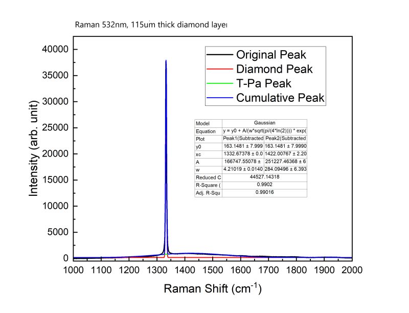
Representative Raman spectrum at 532 nm for a 115 micron thick CVD diamond layer. The diamond peak is centered near 1332 cm-1.
For diamond-on-silicon and related stacks, BEN is intended to improve adhesion, reduce particles and voids, and enable lower thermal boundary resistance compared with mechanically seeded films. In suitable stacks, the development target is substantially higher thermal boundary conductance than conventional seeded interfaces, with independent characterization recommended for customer-specific material systems.
Carat Systems is open to collaborations with device integrators and metrology groups to independently characterize BEN-enabled diamond stacks.